Episode Details
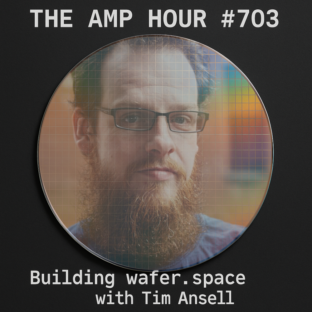
Back to Episodes#703 – Building wafer.space with Tim Ansell
Published 6 months, 1 week ago
Description

Welcome back Tim Ansell!
- Tim’s past appearances and previous work
- Discussing Tomu on 375
- Discussing Fomu on 456.3
- Discussing the open source PDK on 501
- Tim’s previous work at Google involved releasing a manufacturable open-source PDK (Process Development Kit), which contains the fundamental information needed to create integrated circuits.
- Key open-source tools discussed include OpenROAD (a backend compiler for IC design) and Open Lane (an end-to-end suite turning chip descriptions (RTL) into manufacturing data (GDS)). Andreas had been on the show talking about his work on OpenROAD. Not discussed on the show but after Efabless went away, Open Lane has been replaced with LibreLane.
- Efabless, a VC-backed startup, shut down in early 2025 due to investor disagreements. Efabless previously provided pooled manufacturing access (similar to OSH Park for PCBs) using the SKY130 process from Skywater in Minnesota.
- A Skywater run costs $200k–$300k, which Efabless divided by 40 to reach roughly a $10k price point per slot.
- Tiny Tapeout
- Matt Venn’s Tiny Tapeout program further subdivides the manufacturing costs, making it the cheapest way to create custom silicon, typically costing around $300 per design.
- Tiny Tapeout lowers the barrier to entry, allowing people to “just try it and see if you like it,” similar to writing a “hello world” program.
- The program has already processed almost 3,000 projects, demonstrating high community demand when costs are low.
- Despite limitations, advanced projects are possible: a developer taped out a Linux capable SOC using open-source tools and the Tiny Tapeout space.
- Introducing Wafer Space
- Tim started Wafer Space, based in Singapore, to provide community access to open-source manufacturing after Efabless ceased operations.
- Wafer Space focuses on the GF180MCU PDK (Global Foundries 180 nm process), which is a much cheaper technology manufactured in Singapore.
- The core offering is a low-volume production run: $7,000 USD gets you 1,000 chips back. This volume is enough for prototyping and shipping a small product (e.g., 500 units).
- The design envelope area is 3.8 x 5 mm (20 mm squared) using the 180 nm process.
- Interested parties should sign up via the Crowd Supply page. The deadline for purchase is the November 28th and submissions are due by December 3rd, with delivery by March 15th.
- Manufacturing & Packaging
- By defau